Board
The next step in my project was to design the board. The main electronic components I settled for are:
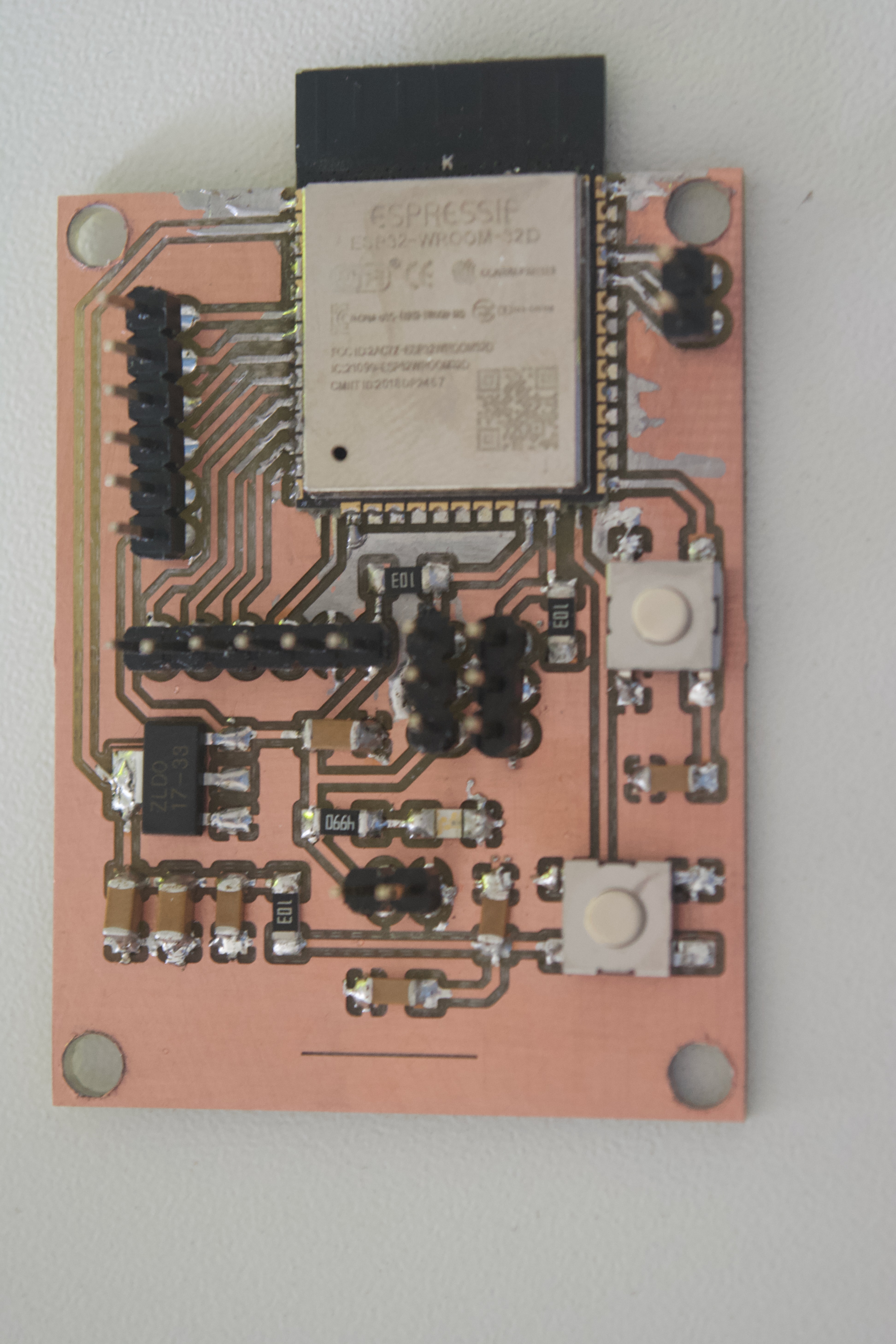
- ESP32 microcontroller (for wireless connectivity)
- 2x 28BYJ48 stepper motors
- 2x ULN2003 driver ICs to control the stepper motors
- 2x Hall effect sensors
All of the design files can be found here.
Schematics
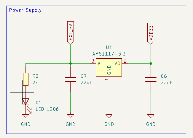
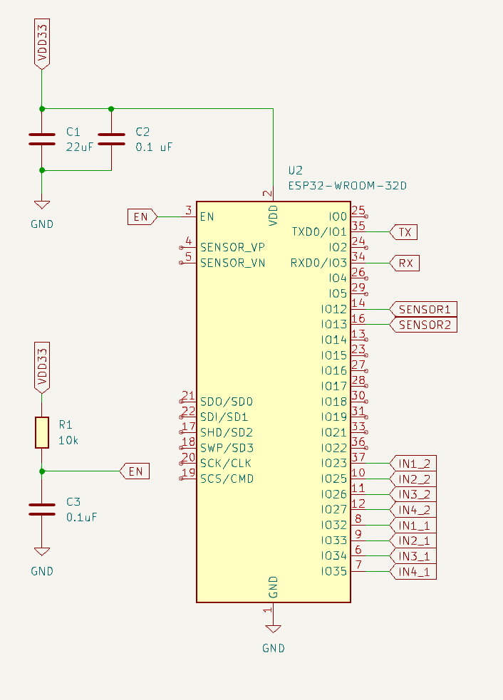
The first step was to determine the power requirements of all the components. I found that the ESP32 requires 3.3V while the stepper motors and Hall effect sensors require 5V. Consequently, I needed a voltage regulator to step down the 5V to 3.3V. I opted for the AMS1117 and included a power LED and a pair of capacitors to stabilize the power output.
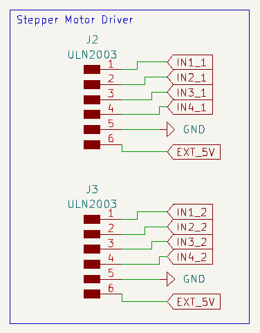
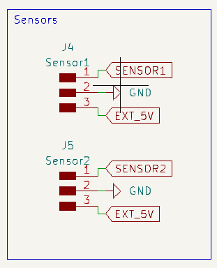
The subsequent step involved adding all the necessary pins/pads to connect the sensors/drivers and to program the microcontroller.

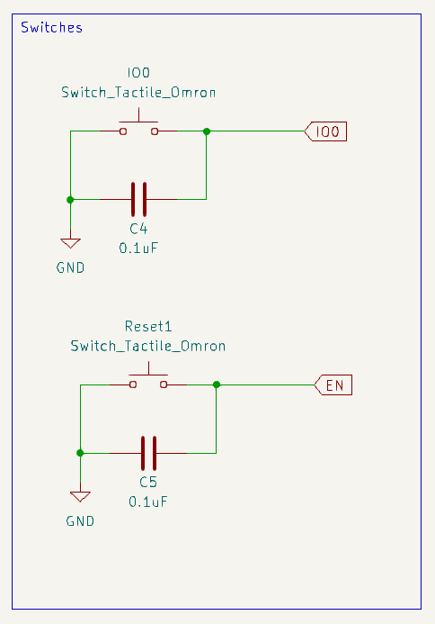
The ESP32 also features two pins that can be used to reset/power cycle the chip and to enter bootloader mode. During normal operation, the "IO0" pin is pulled high (connected to VCC). However, if you ground the "IO0" pin during boot, it will activate the bootloader mode, which allows you to flash new firmware onto the ESP32.
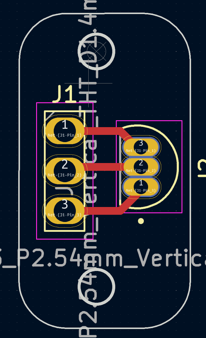
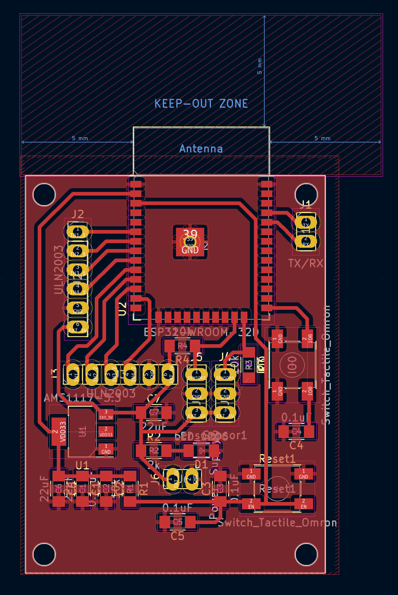
PCB
It was important to keep the antenna of the ESP32 away from the board to prevent interference with the copper or other traces on the board. The GND patch in the middle of the ESP also had several 0.2 mm holes, which I removed since the milling machine lacked the appropriate tools and they were unnecessary anyway. Additionally, I added four mounting holes to the board for easier installation.
Soldering
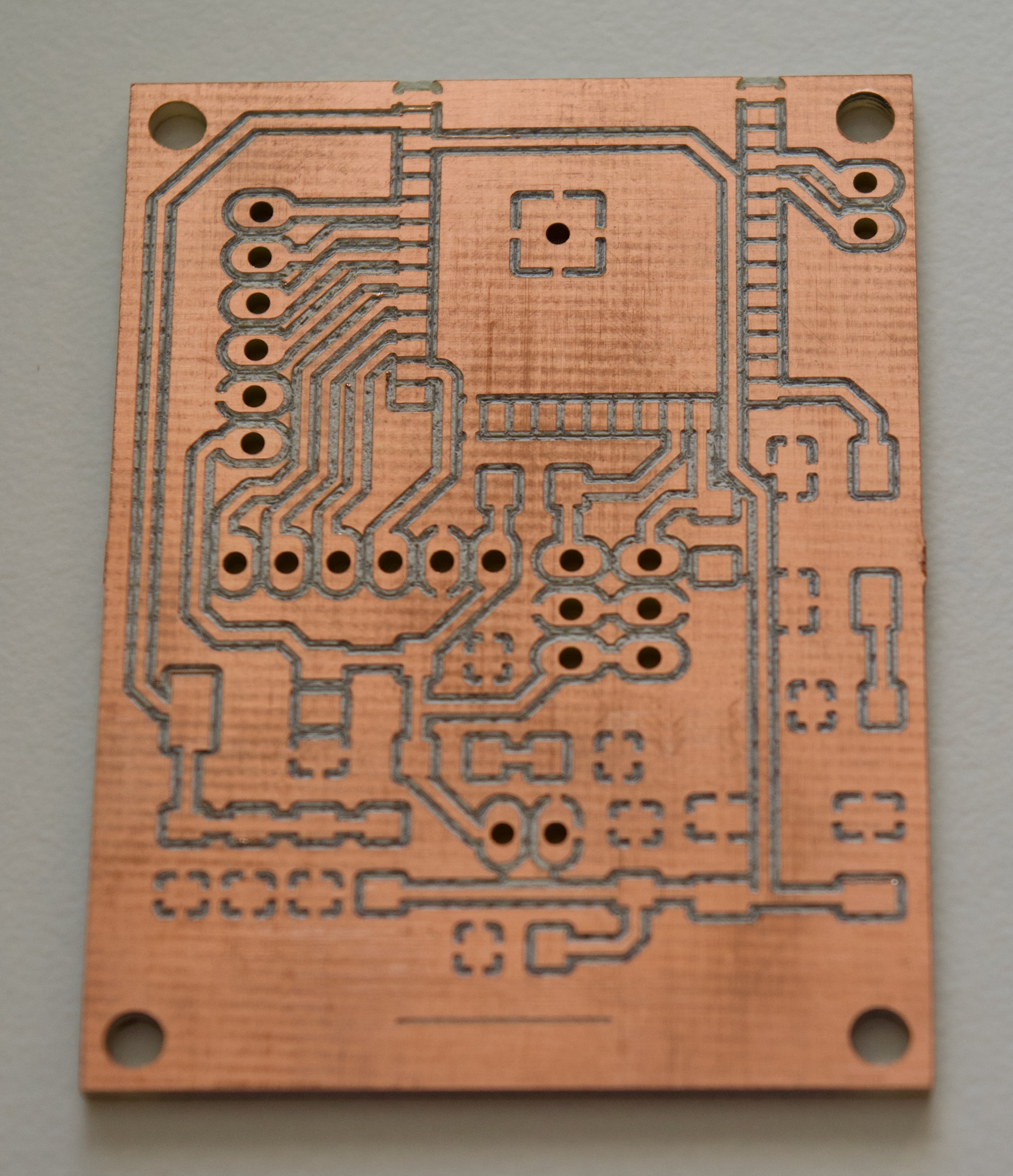
This is what the milled board looked like.
This is what the board looks like after soldering.
Second board
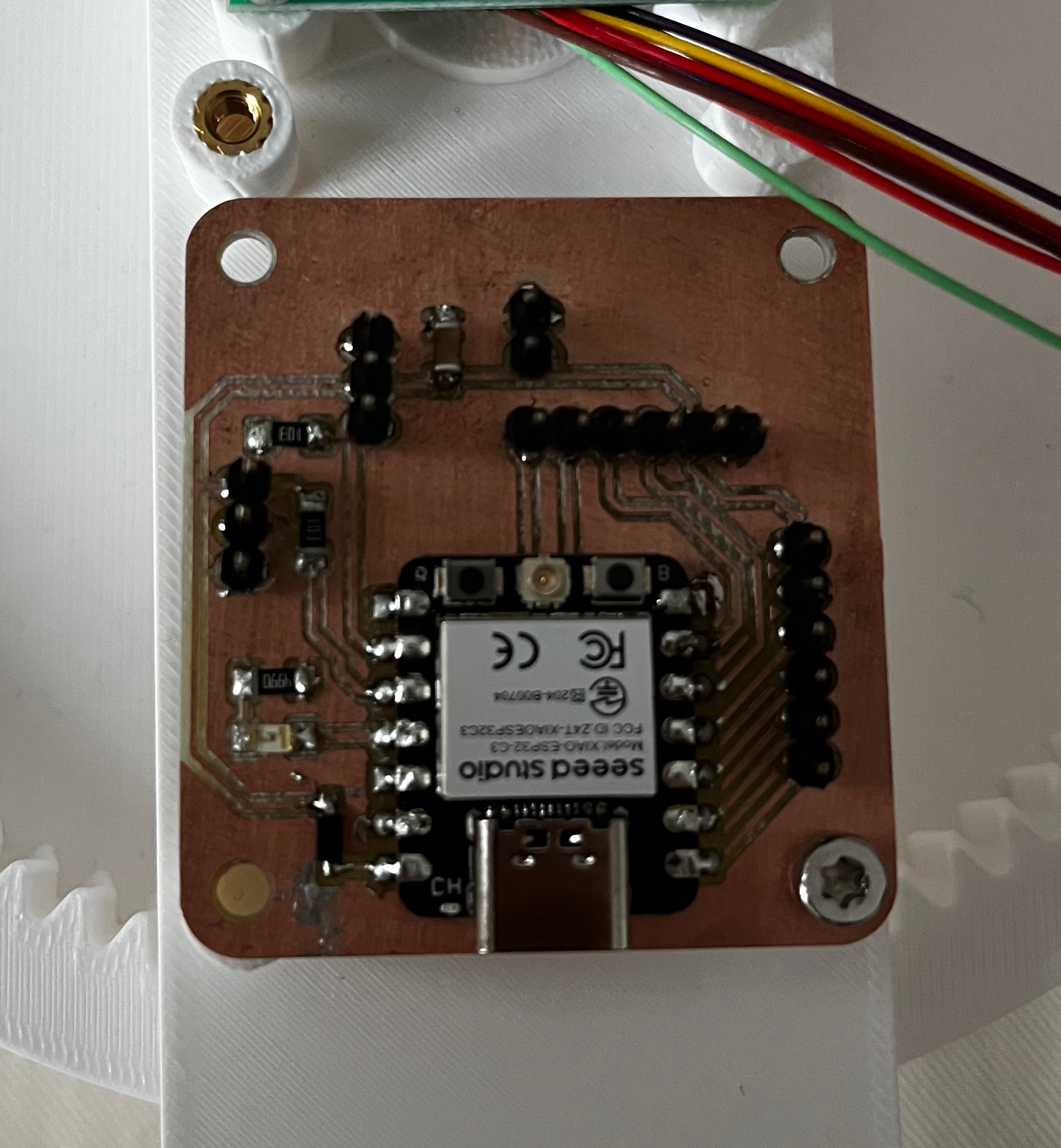
Unfortunately, the first board I created encountered issues. Although I was able to connect to it and successfully flash it once, it ceased to function for reasons that remain unclear. In an effort to conserve time, I decided to use a pre-manufactured ESP32 development board, specifically the XIAO ESP32C3. This board was then soldered onto another board alongside several additional components, including resistors for the sensors, an LED, a capacitor, a diode to manage the 5V input, and several connector pins. All of the design files can be found here.
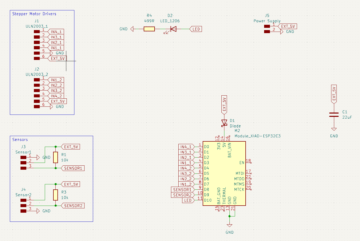
Schematics
Below are the schematics for the second board, illustrating the layout and connections of the various components:
PCB
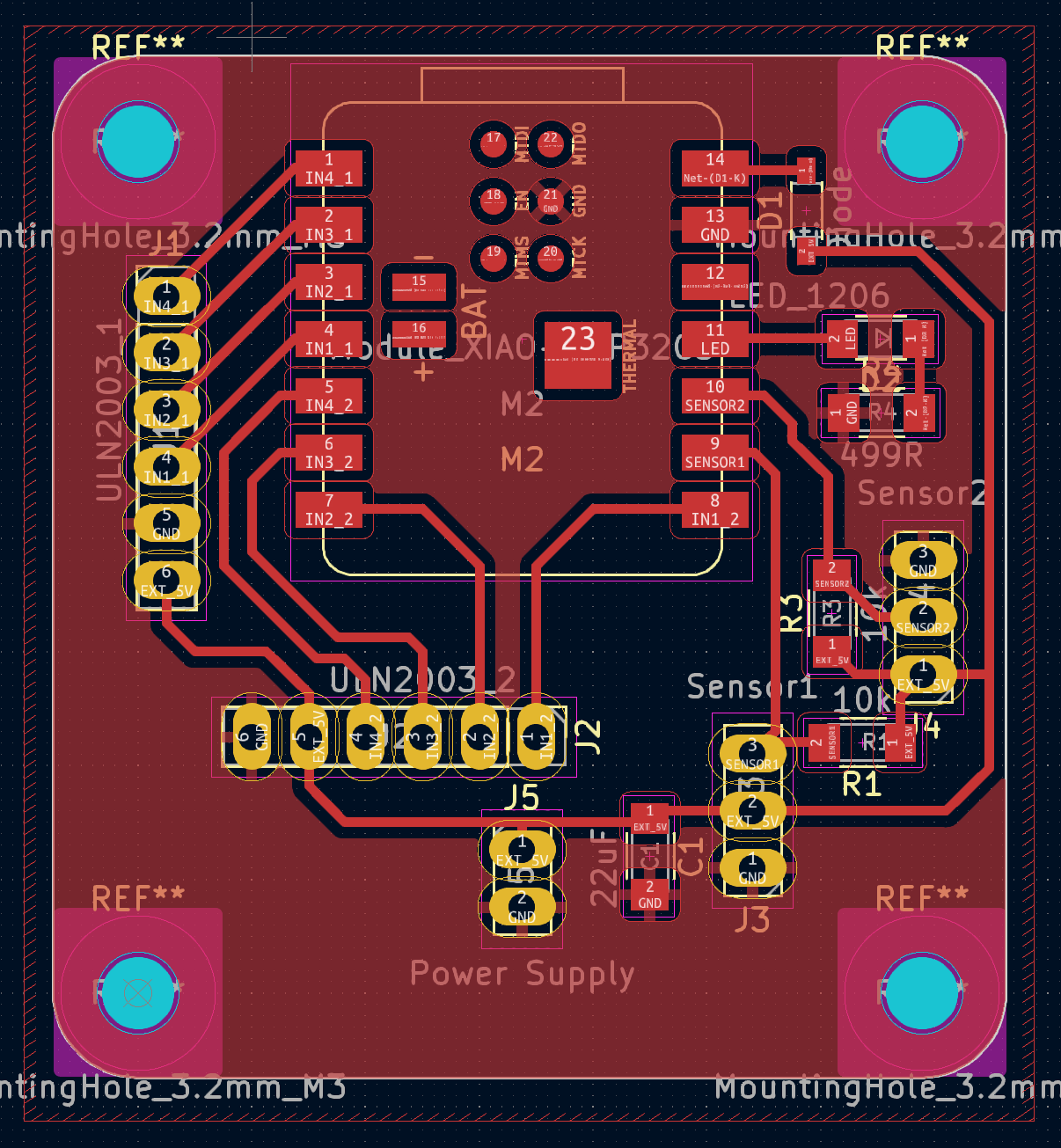
The following image shows the PCB layout, providing a visual guide to the arrangement of components on the board:
Soldering
Soldering the breakout board proved to be significantly easier than soldering the chip directly. Here's the final soldered assembly:
Hall effect sensor board
I also needed to create a simple breakout board for the Hall effect sensors, as directly soldering wires to the sensors proved to be challenging. This board has three pins for connecting cables and three holes for securely mounting the sensor. I was unable to obtain clear images of the boards as my camera is not equipped to focus on such small objects. The design files can be found here.